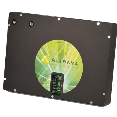
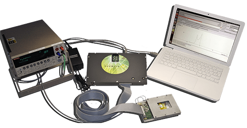
ALIBAVA SYSTEM is a portable and compact readout system for microstrip sensor characterization

This system uses a front-end readout chip, which was developed for the LHC experiments to read out microstrip detectors.
Also enables the user to characterize each individual strip of silicon microstrip sensors beyond CV and IV curves. It provides information such as the Charge Collection Efficiency (CCE), time profile, real time display of the events in each channel, temperature, and many more.
The system is suitable to characterize the properties of irradiated and un-irradiated microstrip sensors. The system hardware has two main parts: a daughter board hosting the readout and a mother board.
The first one contains two readout chips and has fan-ins and sensor support to interface the sensors.
The last one is intended to process the analogue data that comes from the readout chips and from external trigger signals, to control the whole system and to communicate with a PC via USB.
Features
- Calibration, laser or radiation source modes
- Connectivity USB 2.0
- Acquisition software for Windows, Linux and supported Mac
- Chip BEETLE at 40 MHz
- Energy resolution: 3 to 6 KeV
- Energy range: up to 330 KeV
- Trigger mode: 3 external inputs and 1 output.
- External trigger and autotrigger boards available.
- Data stored in custom binary and HDF5 files
- Example macros for further in-depth analysisprovided
- Mother Board dimensions: 250x175x33 mm3
- Daughter Board dimensions: 70×85 mm2
Voltage supply: +5 V
- n-type (holes read out).
- p-type (electrons read out).
- Up to 256 input channels.
Different flavours of detector boards are available to accommodate detectors of different sizes. The system is designed to work with a radioactive source setup and laser setup: useful for comparing results with the same detector.
- The system works with laser setup and a β source.
- Irradiated detectors can also be tested.
- There is a Linux and a Windows version for the software.
Data acquired with the system can be easily processed using ROOT framework: some macros already developed.
A schematic of the Alibava System Classic:

This product is sold under license of Spanish National Research Council (CSIC) and University of Valencia (Spain)
STANDARD DAUGHTER BOARD
The detector board accommodates two ASIC chips to read detector signals, a temperature sensor placed close to the chips and the fewest additional components. A 5V supply level is sent from the mother board. This supply level is regulated by two LDO (Low Drop Out) linear regulators for obtaining the dc supply levels required by the readout chips (2.5 V) and the buffer stage (3.3 V). The detector high voltage power supply is supplied directly to the detector board. This supply level is decoupled prior to the detector.

For this system the ASIC chip analogue output onto one port is used. In this case the analogue front-end pulse signal is sampled into the pipeline with the frequency of the ASIC chip clock (40 MHz). The peak voltage of the front-end pulse signal is proportional to the collected charge at the detector channel, the peak time of this signal is about 25 ns (depending on the load capacitance among other parameters) and the remainder of the peak voltage after 25 ns is below 30% (i.e. the ratio between the signal voltage 25 ns after the peak and the peak voltage). Therefore, a 65–70 ns pulse length is considered in order to reconstruct the pulse. For reading out a particular position of the pipeline, a pulse of 25 ns (TRIGGER) is generated by the mother board.
This pulse is sampled with the falling edge of the readout chip clock (CLK). The analogue pipeline latency has been fixed to 128 clock cycles, so this TRIGGER pulse is generated 128 CLK cycles after a particular front-end signal point has been sampled and stored in the pipeline. For the laser setup the TRIGGER pulse is generated for each event (i.e. laser pulse) with a delay programmed by the user regarding the event occurrence. For the radioactive source setup, the TRIGGER pulse is generated with a fixed delay regarding the event occurrence (i.e. a particle crossing the detector) and a time stamp for each event is obtained with a TDC in the mother board. Therefore, just one sample of the analogue pipeline is required per event in both setups. The pulse shape can be reconstructed by acquiring enough number of events.
SOFTWARE
The main task of the system software is controlling the whole system and processing the data acquired from the sensors as well as storing this data with an adequate format in a PC for further processing.
The software has two levels. The low level software deals with the data exchange by USB with the motherboard and with the low level data processing. No driver design is required at this level since the manufacturer of the USB controller provides with a ready-to-use driver (Virtual Com Port Driver). The high level software implements the GUI for the communication between the user and the system, the data monitoring as well as the data output file generation.
The software has been designed initially for running in a Linux operating system. However, a Windows version of the software is envisaged as well. Both the low level software and the high level software have been implemented in the same package and they have been designed using C++. Some macros for the ROOT framework have been developed in order to process the data obtained with the software.
